https://www.fibre-systems.com/feature/developments-data-centres
Developments in data centres
6 February 2023

What are the top trends, challenges and technologies driving data centre networks in 2023 and beyond?

Image credit: Gorodenkoff /Shutterstock.com
The data centre landscape has seen a lot of change over the past few years, with factors such as the move towards hyperscale – now the most common data centre – to the after-effects of the pandemic driving the data centre to become an even more critical asset.
A recent study from BlueWeave Consulting stated that the global data centre market was worth $206.2bn (£166.7bn) in 2021, and it projects growth to $404.9bn by the end of 2028. The study attributed this growth to an increase in the number of data centres following a period of greater investment by governments and large enterprises, as well as the move towards a cloud environment for businesses. The rise of 5G and adoption of artificial intelligence (AI), IoT, machine learning (ML), big data, and more were also cited as factors.
As such, it is more important than ever that data centres are able to overcome the daily challenges that are thrown at them. Telehouse, a UK-based colocation provider, said it witnessed a number of trends last year that will continue to have an impact on decision-making when it comes to infrastructure. Unsurprisingly, sustainability places highly among these, thanks to carbon reduction targets and more scrutiny on sustainability initiatives. However, a Telehouse survey targeting UK IT decision-makers found that about 34% of organisations have yet to make progress on their sustainability goals. Responses also indicated that 57% of UK businesses are not fully optimised to contribute to net-zero targets, are not using renewable energy sources (52%), and do not closely monitor their carbon footprint (52%).
Growing carbon efficiency demands are making it vital for companies to evolve their working practicesNick Layzell, Customer Success Director at Telehouse Europe, says: “Growing carbon efficiency demands are making it vital for companies to evolve their working practices. There is a real drive for businesses to take more responsibility for all their IT operations – from manufacturing processes to supply chains – and to focus on using green materials, renewable energy, and recycled equipment. Therefore, a cloud-based, data-driven approach, underpinned by the implementation of energy-efficient technologies and digital solutions, will play a critical role in achieving the goal of net zero and furthering business growth.”
Under pressure
Telehouse predicts that hybrid working will increase, and with it the volume of data that needs to be managed. It believes this will put pressure on infrastructure – many data centres have already migrated to 400G and 800G networks, and the move towards 1.6T is imminent. This will likely see more businesses embracing cloud connectivity to provide remote employees with reliable access to data. The move towards colocation data centres will also continue.
Telehouse also envisages AI and robotics becoming more commonplace. The company’s research found that AI adoption grew in 2022, with more than 35% of global companies now using AI in their business, and an additional 42% stating that they are exploring its use. AI and ML tools can help to automate data processes and eradicate human errors.
Operators and users of data centres have a clear responsibility to protect the data that they hold and processA particularly worrying trend for data centres is the likelihood of increased cyber threats, meaning that data centres must implement new security solutions. Ian Levy, Technical Director at the National Cyber Security Centre (NCSC), part of GCHQ says: “Operators and users of data centres have a clear responsibility to protect the data that they hold and process – failing to do this poses a massive financial, reputational and, in some cases, national security risk.”
From a technology standpoint, operators must decide on the best components and systems to help protect the valuable network data while at rest at the data centre. Encryption at the optical layer and optical steganography for data-hiding both offer a high level of protection. Likewise, strong and bend-resistant bre can help to prevent hackers from gaining access via the light leakage that can occur in bends. There has also been a move towards chip-level security, and in more recent years, quantum security products and ML techniques, to safeguard the hardware and so ware.
This journey towards pluggables with optical system-on-chip has also been integral to the deployment of the smaller edge data centres that sit close to the edge of a network. ese have seen significant growth over the past couple of years and this looks likely to continue. In fact, market intelligence firm Spherical Insights predicts that the edge data centre market will reach $31.6bn by 2023, from $5.9bn in 2021.
Harald Graber, Chief Commercial Officer at Effect Photonics, told a market focus session at the most recent ECOC conference and exhibition: “When we talk about edge data centre infrastructure and where this is going, it’s one of the new elds where you have high growth rates in a very exponential dimension.”
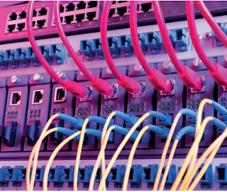
Image credit: asharkyu/Shutterstock.com
Volume production
With these high growth rates, said Graber, will come the need for higher-volume production technologies, and the location will also come into play. “It could be anywhere,” he said. “It can be closer to the enterprise or closer to residential areas if you want to have a cloud edge centre there or closer to certain hotspots on the mobile device, so that’s not really a dependency on the end access requirement, it just drops out further. Then, the question is, what are the data speeds there? As we know, it is different from the core, where performance is a driving factor – access is all about power consumption cost. The edge also has slightly different requirements in terms of data rates and of course in terms of power consumption it’s a bit more stringent than within the main data centres.”
Looking at the back story of the edge and access networks from a technology standpoint, Graber highlighted that there was historically a lot of demand for direct detect technology, which changes the amplitude of the light to transmit information. “There’s still a lot of demand for direct detect like 10G,” he said, “but when it comes to alternatives, the question was always ‘can you make coherent?’ Technically, yes but… e ‘but’ is that the moment I have a coherent module I need a digital signal processor (DSP), and the DSP means I have high power consumption, which is not something you want to have in the access.”
Another challenge with coherent technology for edge data centres, according to Graber, is cost. “We all know with DSPs, there are not too many suppliers out there and so it adds a significant burden on the cost side. A coherent module, if you look at the build-up at least in the classical way, is very complex to manufacture, so there is a ceiling on what can be done. Some market numbers are driven not so much by the market, but more by what the supply can be at this time, so there’s a constrained situation.”
In terms of a solution, Graber highlighted some of the research and development work taking place in the industry to overcome this challenge. “We have seen some announcements, for example, on a 100G ZR DSP coming out with low power for QSFP28, so people are looking into it. We have to fix a problem in the access or in the cloud edge, because, what do you do if you need a 40 or 80km link on 10G? You need more capacity. At some stage there needs to be a solution.”
Technological solutions
Technological approaches to this solution, said Graber, include the development of multi-laser arrays, a move towards full integration, DSP optimisation for indium phosphide, and designing for the existing ecosystem.
Looking at multi-laser arrays, Graber highlighted some successful research from Intel Labs. The company demonstrated an eight-wavelength distributed feedback (DFB) laser array that is fully integrated on a silicon wafer, with output power uniformity of +/- 0.25 decibel (dB) and wavelength spacing uniformity of ±6.5. The array was designed and fabricated using Intel’s commercial 300mm hybrid silicon photonics platform, which is used to manufacture production optical transceivers in volume. It is thought that this could mark a significant advancement in the capabilities of laser manufacturing in a high-volume complementary metal oxide-semiconductor (CMOS) fab by using the same lithography technology used to manufacture 300mm silicon wafers.
Intel used advanced lithography to de ne the waveguide gratings in silicon prior to the III-V wafer bonding process. It found that this technique provided better wavelength uniformity compared with conventional semiconductor lasers manufactured in 3- or 4-inch III-V wafer fabrications. e research could enable production of the optical source with the required performance for future high-volume applications. Grabe posed: “When you start integrating on a chip you can optimise multi-laser arrays’ power consumption, so the question is, do you push for high baud rights or do you go for multilaser arrays?”
Today still we have a lot of discrete buildups on the coherent side, that’s why you have the gold boxing. It’s a piece of art and every engineer loves it. But it’s also very expensive, so full integration would be one option to address itWhen it comes to integration, Graber explained: “Today still we have a lot of discrete buildups on the coherent side, that’s why you have the gold boxing. It’s a piece of art and every engineer loves it. But it’s also very expensive, so full integration would be one option to address it. In addition, today, if you buy a DSP, usually to sell it to somebody who has an internal vertical integration, they have their own silicon photonics programme. They then buy the laser and put the modules together. So, all the DSPs are optimised for silicon photonics.”
Fabrication materials
Discussing a move towards indium phosphide, Graber highlighted how each fabrication material has its own pros and cons, and the DSP can play a role in “taking care” of any weaknesses when it comes to silicon photonics for a more optimised solution. Indium phosphide, however, presents a different set of strengths and weaknesses. For example, it has a much higher output power on the transmit side, but less so on the receive side. “What has not been done so far,” revealed Graber, “and which provides a huge opportunity for improvements in the future, is optimising DSPs for indium phosphide. at is an untapped research area to go even further in the performance and power consumption optimisation”
Building a culture of designing for the existing ecosystem, said Graber, could help to drive down the cost and increase volume production. Offering some examples of the options available, he said: “If we go very simple and say, okay I want to go to 1.6T, I can have a high baud rate at 1.6T, that’s clear. I can have four 400G modules, that’s easy, I can buy that so the complexity is medium. Faceplate density is low, but I need an external multiplexer. Installation-wise, the power loss is not perfect, but you can go ahead and deploy it immediately. Then you have high baud rates, the other extreme. The complexity here is extremely high and if you want to make a DSP, that will involve a lot of upfront investment. e faceplate density will also be high, but you don’t need external multiplexers.”
The other example Graber offered was the use of one module, but with four times 400G, allowing for lower complexity. In this scenario too, the faceplate density is high, but there is no need for an external multiplexer. He said: “If you ask me where it is going, I don’t know. There are always pros and cons of things like certain cost items, power consumption and what you are looking for. We will see a trend that the straightforward one times 100G, one times 400G, one times 800G or 1.6T or 3.2T will probably break apart and we’ll see more solutions going to a two times 800G, four times 400G or four times 800G, maybe for 3.2T, for example. This means that the laser will become more important in terms of how to integrate it so that it is very small in your system.”
Graber highlighted the development of Apple’s M1 chip as a comparison, demonstrating how the electronics industry has worked to overcome a similar problem. The chip introduced a system-on-a-chip architecture, meaning that, instead of having all the functions such as the GPUs, RAM and CPU separate, they are integrated onto a single chip, therefore removing a lot of intra-connection losses. is increases performance while also dramatically reducing the power consumption. Apple has more recently announced the launch of the next generation of this chip, in the M2 Pro and M2 Max. Graber said: “We are on the photonics side, but we can learn from the electronics industry when it comes to this kind of high integration.”